|
Optoelectronics materials
2024-04-07

Assistant instructor Ayoub Yousef Ahmed
Upper Euphrates Basin Developing Centre – University of Anbar
Optoelectronics is one of the branches of electronics, as it deals with light mainly in terms of light emission, sensing and detection, such as (LED) lamps, solar cells, transistors and photodetectors, these devices or electronic parts are made of materials such as (silicon, MWCNTs, SWCNTs and graphene) as it has the possibility to convert (light) or solar radiation falling on it into electrical energy or vice versa. In this scientific article, we will review some optoelectronic materials, in particular graphene, which represents one of the latest episodes of modern exploration of carbon materials (graphite, fullerene, CNT, MWCNTs, SWCNTs and graphene. Carbon is available in nature as a source of graphite, fullerene, carbon nanotubes and graphene. Raman Spectroscopy and its development after laser discovery have helped advance studies of carbonaceous materials, especially graphene. They are able to provide us with a lot of information and details, for example, graphene thickness and conductivity.
Carbons have gone through multiple stages of exploration from the 1960s, when graphite emerged as discovered by Arthur Moore et al. In 1985, C60 was discovered with zero dimensions by Kroto et al, who were awarded the Nobel Prize in Chemistry in 1996.
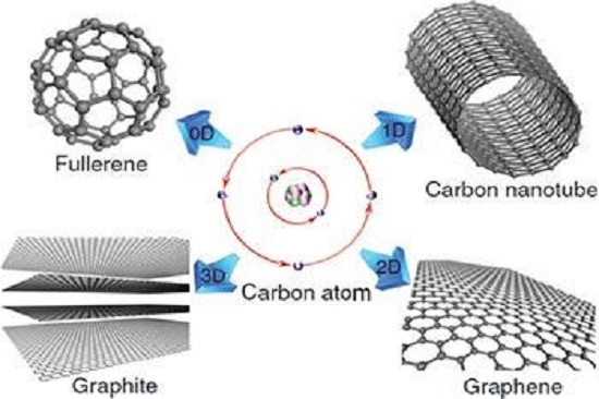
Some materials derived from the carbon atom
The discovery of fullerene (C60) gave impetus to scientists to move forward in research and development, and since this date the number of researchers in this field has been increasing. Research results in 1991 found one-dimension carbon nanotubes (CNT) by Iijima.
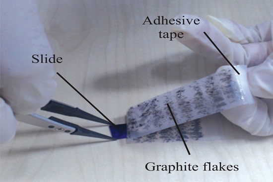
CNTs are the regularity of graphene in single, double, multilayer and wrapped around itself. So-called SWCNTs, DWCNTs, and MWCNTs) result in unparalleled properties that may be valuable in a wide range of uses such as electronic and optoelectronic uses. Research scientists and researchers continued their research until it saw the light and found SWNTs in 1993. The researchers continued their research until 2004, when Novoselov et al. revealed a two-dimensional material, graphene, which comes with one layer, which is equal to one atom of graphite, which was a hexagonal lattice that was obtained in a simplified and primitive way, and this method includes using a piece of adhesive tape to remove graphite chips from a sheet of graphite at that time. The foil is exfoliated using more adhesive tape and applied to more silica strips until a one-atom-thick layer of graphite, i.e. graphene, is finally left fixed to the chip.
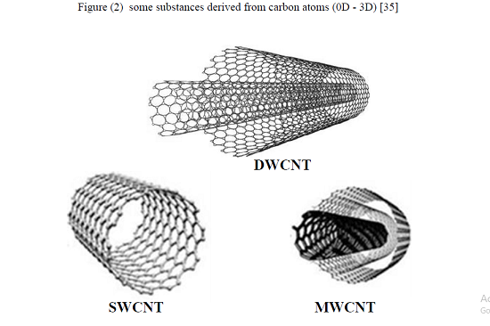
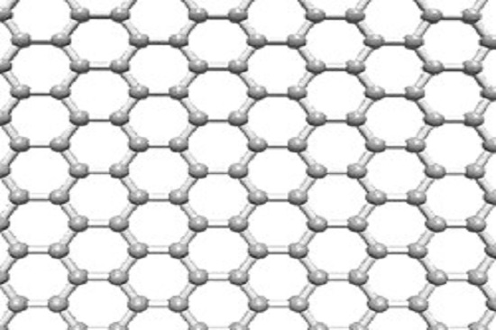
Single-walled, double-walled and multi-walled nanotubes Hexagonal carbon lattice structure for graphene
Other methods of graphene production exist but are less commonly used, including methods for producing up to 30 square inches of graphene that include ion implantation, chemical vapour deposition, liquid-phase exfoliation, and epitaxial growth upon a silicon carbide substrate. Graphene has gained great interest recently among scientists and researchers because it has distinctive properties and potential with Nano electronic uses or applications. Therefore, it is a fast-rising star and has become a shining star among materials. The number of academic publications on graphene use was so large that in 2013 it was estimated at more than 40 publications per day. Previous studies have shown that graphene not only has high conductivity at normal temperature, as the charge carrier in graphene is extremely high and can be used in transistor applications (FETs). It also has a lot of distinctive properties such as optical transparency up to 97.7% and flexibility These properties have potential benefits for transparent electrodes in solar cell applications and even three-dimensional data storage and other properties that can be used in the manufacture of electronic components that have added to this field multiple properties for future devices. Add to this the great mechanical features and high thermal conductivity features.
#university_of_anbar
#Upper_Euphrates_Basin_Developing_Center
References:
1- A master’s thesis - May 2017 (analysis of optoelectronics materials) Ayoob yousif ahmed alqurqash.
2- Materials Today - Volume 17, Number 9 - November 2014 (A decade of graphene research: production, applications and outlook) Edward P. Randviir, Dale A.C. Brownson and Craig E. Banks. |